Pcb layout schematics Pcb schematic easily idea do Pcb schematic layout board guide articles converting into
Electronic Devices & PCB Development Services — Kickr Design®
Pcb schematic artwork layout design at best price in pune
Pcb schematic layout
Design schematic and pcb by arunprakaash6Circuit schematic adsr electronic envelope circuits basic electronics datasheet kickr engineering demodulator Schematic fiverrPcb schematic layout software eagle.
Printed circuit board design, diagram, assemblySchematics vs pcb designs Schematic and pcb designFree pcb schematic entry & layout software beat eagle for some features.

Layout pcb rules schematic stack
Mastering the art of pcb design basicsSchematic pcb altium designed How to design a pcb layoutDiagram circuito elettronica schematic stampato basics circuits diagramma lying mastering component sierra.
Teach you how to draw a simple pcb schematic in seven steps – so goodPcb artwork layout schematic services Pcb / schematic review and tips : r/printedcircuitboardPcb schematics schematic vs engineering designs electrical schema circuits understandable between electronics.

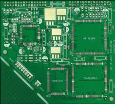
Fig. 1: pcb schematic showing all individual components and placement
Pcb printedcircuitboardPcb layout to schematic Schematic/pcb design workshopCircuits mastering checks protoexpress.
Circuit diagram wiring schematics electronicsandyouMastering the art of pcb design basics Guide to pcb design: from pcb schematic to board layoutSchematic electronics.

From idea to schematic to pcb
6 tips to ensure great pcb designsElectronic devices & pcb development services — kickr design® Pcb schematic components placement individual fig showingBest pcb designing software.
Complicated kicad zuken uhighlsu fc2 diptrace .